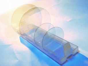


Silicon Carbide Wafers Industrialization Base Project has been started construction!
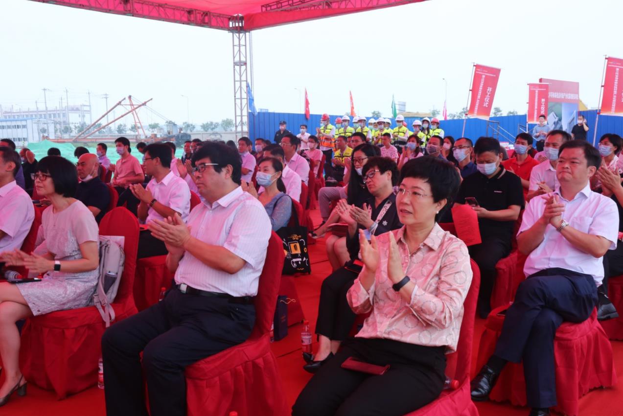
On August 17, 2020,a foundation stone lying ceremony of Tankeblue's Silicon Carbide Wafers Industrialization Base Project was held in the southeast industrial zone of Daxing District, Beijing, China. Some government leaders and guests attended the ceremony.
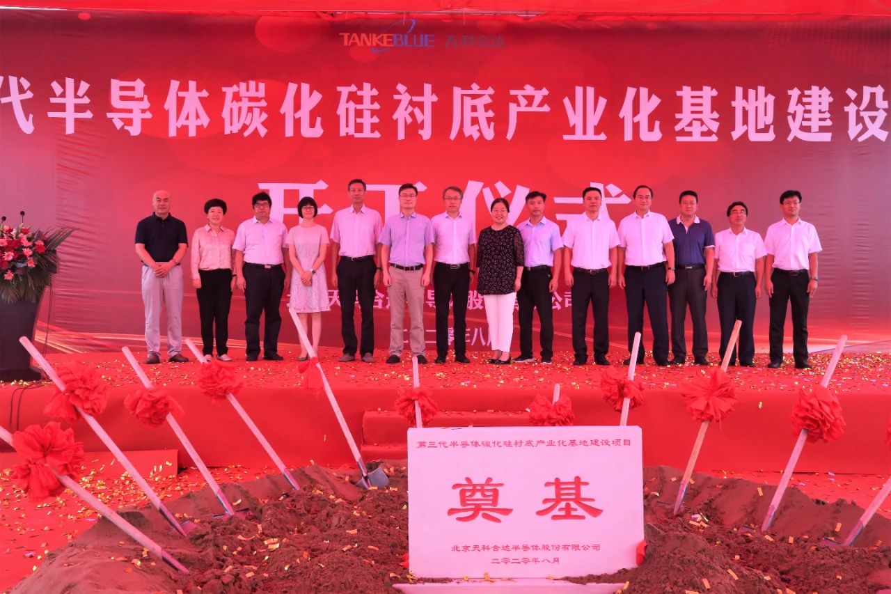
Yang Jian, general manager of Tankeblue Semiconductor Co., Ltd., expressed his heartfelt thanks to the leaders, cooperative partner and cooperation units who care about and support the project. Mr. Yang said that Tankeblue will be committed to building a leading enterprise in the world for the wide band-gap semiconductor silicon carbide wafer materials, so as to provide strong support for the development of China's wide band-gap semiconductor silicon carbide industry. Some leaders attended and delivered speeches.
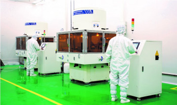
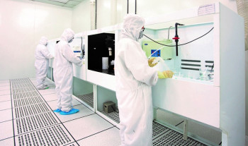
The total investment of silicon carbide wafers industrialization base project is about 950 million yuan, with a total construction area of 55000 square meters. A new silicon carbide wafer production line with 400 sets of monocrystalline silicon carbide growth furnace and its supporting cutting, grinding and polishing equipment is planned to be completed and put into production in early 2022. After completion, the silicon carbide wafer production line can produce 120000 silicon carbide wafers annually.